- Home
- Computing
Computing
About
News, reviews, and discussion about desktop PCs, laptops, and everything else in the world of computing, including in-depth buying guides and daily videos.

The 10 best monitors for 2024: tested and reviewed


How to do a hanging indent in Microsoft Word
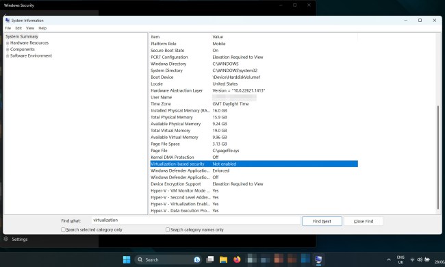
How to disable VBS in Windows 11 to improve gaming

How to do hanging indent on Google Docs
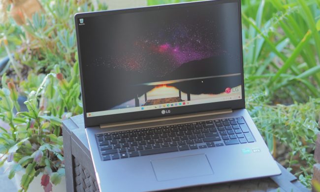
LG just knocked $300 off this 16-inch lightweight laptop


How to download a video from Facebook
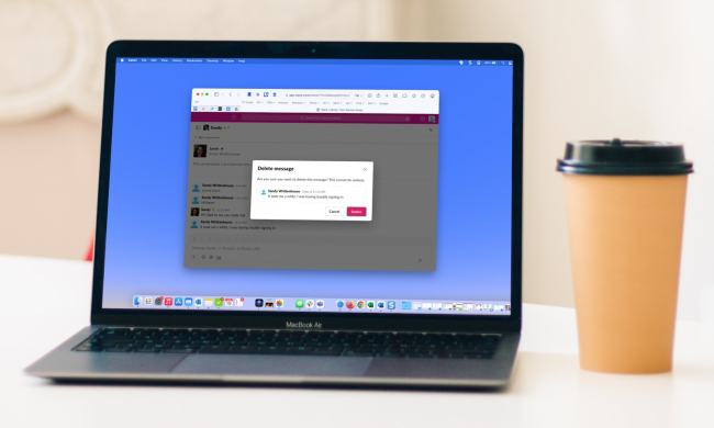
How to delete Slack messages on desktop and mobile
I finally found a gaming laptop utility that’s actually worth using
How to download Vimeo videos on desktop and mobile

Hurry! The Razer Blade 17 gaming laptop is 44% off today
How to dual boot Linux and Windows

How to change mouse DPI on Windows and Mac
How to choose an external hard drive

Meta has a bold new strategy for VR
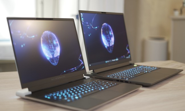
Alienware m16 R2 vs. Alienware x16 R2: Which 16-inch model is better?
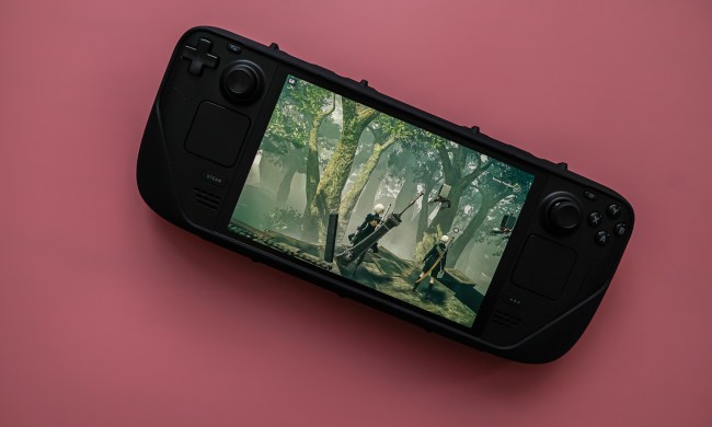
Buying a Steam Deck has never been cheaper

The Vision Pro is already in trouble. Here’s how Apple can turn the tide

The MSI Claw just got both faster and cheaper

VR is even cheaper: Meta Quest 2 just got a price reduction
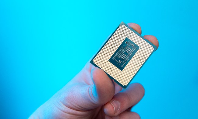
Some Intel CPUs lost 9% of their performance almost overnight

Quick! This Lenovo ThinkPad X1 Yoga 2-in-1 laptop is 51% off
How to type an em dash on a Mac

One of HP’s best 2-in-1 laptops just had its price slashed to $460
Computing News


Laptops


Computing Reviews


Nvidia


For those seeking a superior computer setup, a cutting-edge monitor is non-negotiable. Whether you're entrenched in graphic design, a dedicated gamer, or a remote professional, the right display has the power to transform your computing experience. With a myriad of options available, ranging from various resolutions and panel types to refresh rates and specialized features, navigating the world of monitors can be overwhelming.
Investing in a good PC monitor can enhance your computing experience in several ways:
Visual quality: A high-quality monitor offers superior visual clarity, color accuracy, and sharpness compared to budget or older monitors. This is particularly important for tasks like graphic design, photo editing, and gaming, where color accuracy and detail are crucial.
Resolution and refresh rate: A good monitor often comes with higher resolutions (such as 1440p or 4K) and faster refresh rates (such as 120Hz or 144Hz). This results in a smoother, more immersive gaming experience, reduced motion blur, and improved overall screen performance.
Panel type: Premium monitors often use advanced panel technologies like IPS (In-Plane Switching) or OLED (Organic Light-Emitting Diode) for better color reproduction, wider viewing angles, and deeper blacks. These panels provide a more enjoyable viewing experience for various tasks, including watching videos or working on creative projects.
Productivity and multitasking: A larger, high-resolution monitor enhances productivity by providing more screen real estate for multitasking, running multiple applications side by side, and improving workflow efficiency.
Adaptive sync and gaming features: Many high-end monitors come with features like Nvidia G-Sync or AMD FreeSync, which synchronize the monitor's refresh rate with the graphics card's frame rate. This eliminates screen tearing and stuttering, resulting in smoother gameplay for gamers.
Adjustability and ergonomics: Good monitors offer ergonomic features such as height adjustment, tilt, swivel, and pivot, allowing you to customize the viewing angle for comfort and reduced eye strain. This is beneficial for long hours of work or gaming sessions.
Connectivity options: Premium monitors typically offer a wide range of connectivity options, including HDMI, DisplayPort, USB-C, and more. This versatility allows you to connect multiple devices simultaneously and switch between them seamlessly.
Long-term investment: A high-quality monitor is a long-term investment that can last for several years without needing an upgrade. It provides consistent performance and reliability, saving you money in the long run compared to frequently replacing cheaper monitors.
Read on to see which monitors we recommend for gaming, home use, and more.
Dell UltraSharp 32 4K
The best monitor you can buy
- Large, sharp 4K IPS panel
- Excellent image quality
- Truly useful USB-C hub and KVM switch
- Outstanding build quality and design
- Standout warranty and support
- Expensive
- HDR support is so-so
Why you should buy this: It's a gorgeous screen with thin bezels and deep blacks.
Who it’s for: Anyone who wants a premium monitor that will last years.
Why we picked the Dell UltraSharp 32 4K:
Dell's UItraSharp 32 4K isn't the cheapest monitor out there, but it's the best. It offers a balance of beautiful image quality and features that few monitors can nail, and does so at a reasonable price.
We specifically reviewed the 32-inch model, which is more expensive than the 27-inch version (the U2723QE). Most people are fine with the 27-inch version, though the 4K resolution looks its best on a 32-inch panel. Regardless of the size, both monitors use an IPS Black panel, which provides wide color coverage and excellent color accuracy. It's also significantly brighter than a standard IPS panel, offering up about twice the contrast you'd normally find.
Outside of image quality, Dell's UltraSharp 4K displays feature an integrated USB-C hub that's surprisingly useful. It sports up to 90 watts of power delivery, and it gives you a one-cable solution for connecting a laptop to the display. With the single USB-C cord, you can daisy-chain a second monitor, connect to the Ethernet port, and access both DisplayPort and HDMI connections. The monitor even comes with a KVM switch, allowing you to quickly swap your peripherals between devices.

MSI MPG 321URX QD-OLED
The best gaming monitor
- Much cheaper than the competition
- Some of the best color we've seen
- Extensive list of OLED burn-in prevention features
- 1,000 nits of brightness
- 3-year warranty that covers burn-in
- A rather bland design
- Limited to USB 2.0 with integrated hub
Why you should buy this: An exceptionally good OLED gaming monitor with a competitive price tag.
Who it’s for: Gamers who want the most immersive gaming experience.
Why we picked the MSI MPG 321URX QD-OLED:
MSI's MPG 321URX QD-OLED gaming monitor stands out for its exceptional image quality at a lower cost compared to competitors, with an MSRP of $950. The monitor boasts impressive features such as OLED burn-in prevention, 1,000 nits of brightness, and a three-year warranty covering burn-in issues. Despite its pros, including vibrant colors and a reasonable price, it falls short in design aesthetics and is limited to USB 2.0 connectivity with an integrated hub.
The monitor's design is modest, with a plastic shell and a glossy finish that complements its OLED panel. It offers extensive adjustment options, including height, tilt, swivel, and pivot, making it versatile for different setups. While lacking some advanced features found in competitors, such as Black Frame Insertion (BFI), the MPG 321URX excels in image quality, gaming performance, and burn-in prevention features, making it a compelling choice for those seeking a high-quality OLED gaming monitor without breaking the bank.

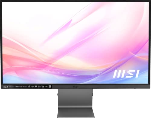
MSI Modern MD271UL
The best cheap 4K monitor
- Excellent colors
- Good brightness and contrast
- Affordable price
- Solid build
- Attractive design
- Confusing buttons
- Limited flexibility
- Ugly marketing label
Why you should buy this: It's a 4K monitor with premium features under $300.
Who it’s for: Those who want a high-resolution display without spending too much.
Why we picked the MSI Modern MD271UL:
In years past, 4K monitors were pricey luxuries, but that's quickly changed. A perfect showcase of that is MSI's Modern MD271UL, which is a 27-inch 4K display that you can find for around $250. There isn't special here, but that's what makes the Modern MD271UL so special. It's a workhorse 4K monitor that comes in at a bargain bin price.
The 4K IPS panel is set with thin bezels, which is set against a stark silver frame. For connectivity, you get two HDMI 2.0b ports, a single DisplayPort 1.2a connection, and a 3.5mm headphone jack. The MD271UL also includes a USB-C input with 65 watts of power delivery, which is a nice bonus on a monitor at this price.
But the MD271UL really earns its stripes in image quality. Based on our testing, the monitor is well-calibrated from the factory, arriving with excellent color accuracy and coverage. It also managed to exceed our typical brightness and contrast thresholds for IPS panels. On cheaper monitors, we typically expect brightness or color to suffer, but the MD271UL manages to miraculously do both.
Alienware 27 QD-OLED
Best OLED monitor
- Exceptional image quality
- Speedy 360Hz refresh rate
- Much-improved color accuracy
- Great cable management solution
- Unmatched OLED warranty
- Bezels are a bit thick
- Smart HDR requires a bit of tweaking
Why you should buy this: It's the best OLED monitor you can buy right now.
Who it’s for: Users who primarily use their PC to consume media.
Why we picked the Alienware 27 QD-OLED:
The Alienware 27 QD-OLED stands out as a remarkable monitor, challenging the likes of LG's UltraGear OLED 27 as one of the best 27-inch OLED options on the market. Priced at $900, it brings several improvements, including third-gen QD-OLED technology that significantly enhances color accuracy and brightness. With a 360Hz refresh rate, the monitor excels in providing an exceptionally smooth gaming experience, making it suitable for both competitive and cinematic titles. The minimalistic design, along with a hexagonal stand and efficient cable management, contribute to an overall premium aesthetic.
The monitor's color accuracy, particularly in the standard picture profile, is exceptional, showcasing a Delta-E of 0.46. It even excels in HDR performance, with a peak brightness of 928 nits, perfect black levels, and infinite contrast, all of which enhance the overall image quality. Despite some concerns about bezel thickness and Smart HDR settings requiring tweaking, the Alienware 27 QD-OLED impresses with its striking design, robust port selection, and improved QD-OLED technology.
The monitor comes with a three-year warranty covering burn-in, setting it apart from competitors and solidifying its position as a market leader in the gaming monitor category. If you are looking for a traditional OLED monitor, the LG UltraGear OLED 27 is also highly recommended, especially at its reduced price of $750.
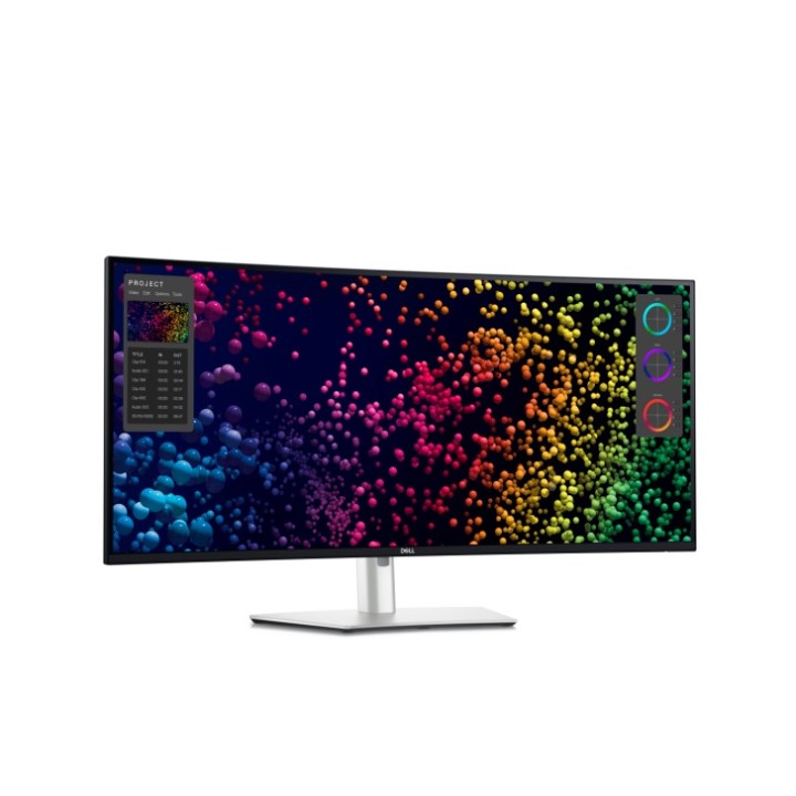
Dell UltraSharp U4025QW
The best 5K monitor
- 120Hz refresh rate
- Network KVM switch
- Great image quality
- Built-in Thunderbolt
- Expensive
- Ultrawide isn't for everyone
Why you should buy this: A high-quality 5K monitor packed with modern I/O.
Who it’s for: Those looking for a premium, high resolution display from enhanced productivity.
Why we picked the Dell UltraSharp U4025QW:
Dell recently unveiled its updated UltraSharp U4021QW 40-inch curved 5K monitor, now available for purchase as the Dell UltraSharp U4025QW 40-inch Curved Thunderbolt hub monitor. Packed with a plethora of I/O options, this monitor supports up to 140 watts of power delivery via Thunderbolt 4, alongside HDMI 2.1, DisplayPort 1.4, an RJ45 Ethernet jack, and various USB ports. It even features pop-down, forward-facing USB ports similar to Dell's 6K UltraSharp monitor.
The monitor's 5K resolution (5120 x 2160) panel has been significantly upgraded, now supporting a smooth 120Hz refresh rate and utilizing IPS Black technology for improved contrast. While it may not achieve the deep blacks of OLED displays, Dell believes it strikes a good balance in contrast. Additional features include an ambient light sensor for automatic brightness and color temperature adjustments, reduced blue light emissions for enhanced eye comfort, and a built-in Network KVM switch for seamless multitasking across multiple network-connected PCs and monitors using a single keyboard and mouse.
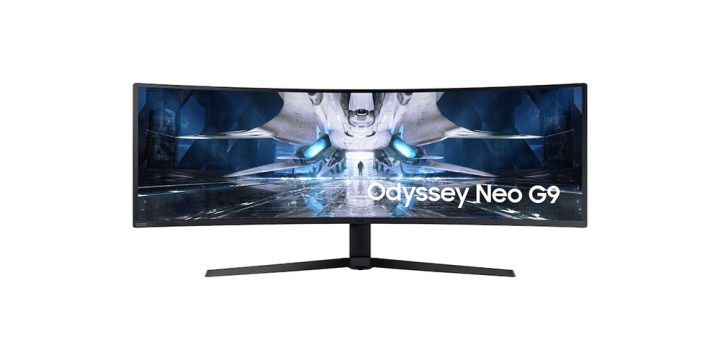
Samsung Odyssey Neo G9
Best ultrawide monitor
- Large 49-inch screen
- Excellent contrast
- HDMI 2.1 support
- Fast response time
- 240Hz refresh rate
- Expensive
- Can be large for some desks
Why you should buy this: A premium ultrawide monitor suitable for all
Who it’s for: Anyone who is looking for plenty of screen real estate.
Why we picked the Samsung Odyssey Neo G9:
The Samsung Odyssey Neo G9 is our pick for the best ultrawide monitor. Featuring a massive 49 inch screen, the monitor features mini-LED backlighting which translates to excellent brightness along with impressive local dimming which helps it display deep blacks. The Odyssey Neo G9 is suitable for most use cases. The sheer size and high-resolution of the screen ensures that you can multitask with ease. It is also great for content creation and media consumption as the panel is capable of reproducing vivid colors with high contrast and deep blacks.
It is primarily a gaming monitor, which means you get all the latest tech including a 240Hz refresh rate and native support for FreeSync variable refresh rate (VRR) technology and G-SYNC compatibility to effectively minimize screen tearing. You also get two HDMI 2.1 inputs to fully capitalize on the latest gaming consoles or graphics cards.
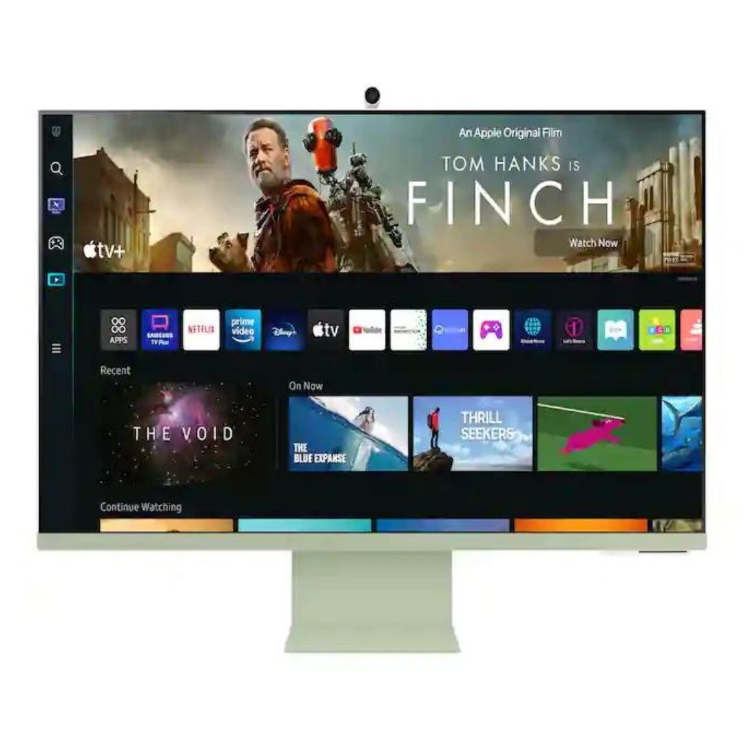
Samsung M8 Smart Monitor
Best smart monitor
- Works as a smart TV or a monitor
- Supports Samsung Gaming Hub
- Attractive design
- 65W USB-C power delivery
- Good SDR image quality
- Limited HDR performance
- No VESA mount and limited stand adjustment
- Webcam features aren't available on a PC
Why you should buy this: A feature-packed monitor that can also be used as a TV.
Who it’s for: Users lacking the room, budget, or inclination for two sizable and costly screens.
Why we picked the Samsung M8 Smart Monitor:
The Samsung M8 Smart Monitor, attempts to bridge the gap between TVs and monitors, offering a versatile solution. Boasting an attractive design with vibrant color options, the M8 resembles the M1 iMac in terms of aesthetics. Its height-adjustable stand and thin bezels contribute to a sleek look. The monitor supports Samsung's TV operating system, Tizen, providing access to apps like Netflix, YouTube, and Apple TV+. While it offers features like Samsung Gaming Hub and Samsung Workspace, the transition between monitor and TV modes is not seamless, making users choose one mode over the other.
With its 32-inch 4K VA panel, the M8 delivers good SDR image quality, but its HDR performance is limited. The monitor lacks VESA mounting options and offers minimal stand adjustments, which may limit flexibility. The bundled magnetic webcam offers good quality and offers features like face tracking and auto-framing. Gaming on the M8 is constrained by its 60Hz refresh rate and a limited port selection, with options like mini HDMI and USB-C. Overall, the Samsung M8 is suitable for those who need its unique combination of TV and monitor functionalities, but alternative options may better cater to specific preferences or use cases.

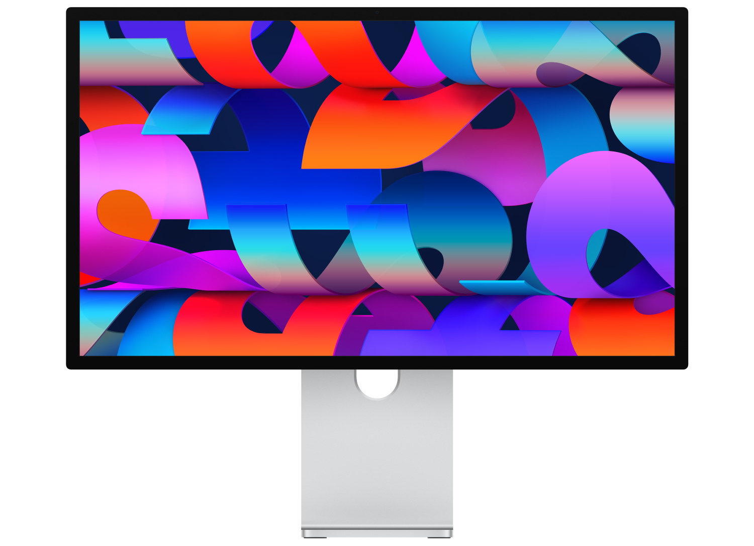
Apple Studio Display
The best monitor for Mac
- Beautiful 5K panel
- Built-in webcam and microphone
- Siri support
- Expensive
- Limited port selection
Why you should buy this: It's a stunning 5K monitor that pairs perfectly with Macs.
Who it’s for: Apple users who want a premium display.
Why we picked the Apple Studio Display:
Apple's Studio Display was a controversial monitor when it first launched, but there's no denying that it's a perfect pairing with any Mac. The 5K Retina display is stunning, offering up 218 pixels per inch on the 27-inch monitor. It also comes with wide color coverage and boasts up to 600 nits of peak brightness.
The display itself is stunning, but the integration with Macs is why the Studio Display topped our list of the best monitors for the Mac mini. The built-in camera and microphone array are tuned for FaceTime calls, and the display even supports Siri commands. The camera also supports Apple's Center Stage to automatically frame you.
For connectivity, you get a Thunderbolt 3 input that provides up to 96 watts of power delivery, along with three downstream USB-C ports. The monitor is built for Macs, but due to the Thunderbolt 3 connection, you can also connect an iPad Pro or iPad Air.

Asus ProArt PA32UCG-K
Best monitor for creative work
- Exceptional color accuracy
- 1600 nits HDR brightness
- 4K resolution with 120Hz refresh rate
- Included hood and light meter
- Very expensive
- Heavy to move
Why you should buy this: A top -class monitor with excellent color accuracy, brightness, and clarity.
Who it’s for: Professionals who need a premium monitor for content creation.
Why we picked the Asus ProArt PA32UCG-K:
The Asus ProArt PA32UCG is a top-tier professional monitor that comes with a hefty $5,000 price tag, but its exceptional performance and comprehensive features justify the investment for professionals. With a 4K resolution (3840 x 2160) and 120Hz refresh rate, this 32-inch monitor is rated to support 100% of sRGB, 99.5% of AdobeRGB, and 98% of DCI-P3 color gamut.
Apart from offering great image quality, the monitor delivers excellent accuracy across various color modes and supports every gamut, grayscale, and gamma standard. Thanks to the inclusion of Dolby Vision support, it further enhances its versatility for professional use. The monitor also comes with essential accessories such as a light hood and color meter, enhancing its appeal for users who demand precise color representation.
With full-array mini-LED backlighting, there are 1152 dimming zones, and the monitor can achieve a peak HDR output of 1600 nits. Its extensive OSD controls allow for fine-tuning of gamma, color temperature, and gamut, ensuring optimal performance tailored to individual preferences. The PA32UCG's exceptional capabilities make it worthwhile for professionals seeking uncompromising accuracy and even gamers craving immersive visual experiences.
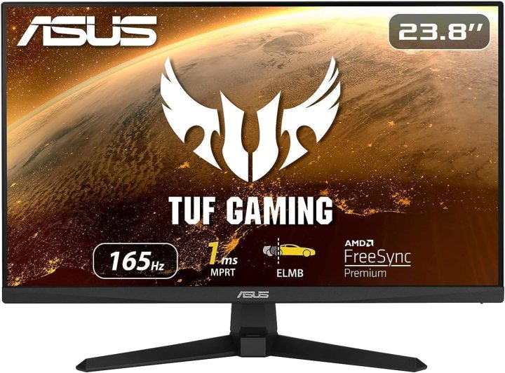
Asus TUF Gaming VG249Q1A
Best 1080p monitor
- Affordable price
- Fast refresh rate and response time
- Good viewing angles
- Small size
- Basic ergonomics
Why you should buy this: A value for the money 1080p gaming monitor that is also good for everyday work
Who it’s for: Users on a tight budget who need a reliable monitor.
Why we picked the Asus TUF Gaming VG249Q1A:
We could recommend a boring office monitor if you need the bare minimum. But the Asus TUF Gaming VG249Q1A is available at an equally competitive price, and on top of that, it offers certain features that can be useful for gamers. It's a decent budget monitor featuring a 24-inch IPS panel with a 1080p resolution and up to a 165Hz refresh rate, plus support for both FreeSync support and G-Sync compatibility.
It isn't the brightest monitor, nor does it offer superior color accuracy due to its limited sRGB coverage, but that's a compromise you need to face with a budget monitor. The monitor comes with relatively good viewing angles and overall it is great for basic productivity and casual gaming.
Frequently Asked Questions
No one monitor brand makes all the best monitors in the world — that’s why this list is populated by a number of different manufacturers. That said, there are some that you can rely on more than most to produce great screens. Dell is a longstanding favorite of ours with years of fantastic displays under its belt. It also tends to cater well to the professional crowd just as much as gamers, so you know there will be something you like in its lineup.
Other noteworthy brands worth considering include Acer, which tends to produce some of the world’s best gaming screens; Samsung, which offers some of the best ultrawide screens and large-size monitors we’ve ever seen; and LG, which has a good all-around catalog of displays.
This very much depends on the resolution you’re targeting and how much desk space you have. While bigger does tend to look better, giving you more screen space for work and larger images for games and movies, they can stretch entry-level resolutions like 1080p to the limits of their clarity. Big screens also require more room on your desk, so we’d caution buying a massive ultrawide like the Samsung Odyssey series if you’re working or playing on a small desk.
As a quick rule of thumb, 1080p looks great up to about 24 inches, while 1440p looks good up to and beyond 30 inches. We wouldn’t recommend a 4K screen any smaller than 27 inches as you aren’t going to see the real benefit of those extra pixels in what is a relatively small space by that resolution.
They can be. 4K offers the pinnacle of gaming detail and, in atmospheric games, can give you a whole new level of immersion, especially on larger displays that can fully display that mass of those pixels in all their glory. These high-res displays really excel in games where frame rates are not as important as visual clarity. That said, we feel that high refresh rate monitors can deliver a better experience (especially in fast-paced games like shooters), and unless you have the deep pockets to splash out on a powerful graphics card or two as well, you aren’t going to get those frame rates at 4K. A 27-inch, 1440p display is still the sweet spot.
Also, keep in mind monitor performance is now often linked to framerate management technologies like FreeSync and G-Sync, so watch for these technologies and compatible graphics cards when making gaming monitor decisions. FreeSync is for AMD graphics cards, while G-Sync only works with Nvidia’s GPUs.
The short answer is they’re both the same. The longer answer is that this is a failure of company marketing in properly conveying what its products are. Today most monitors that use LCD technology are backlit with LEDs, so typically if you’re buying a monitor it’s both an LCD and LED display. For more of an explanation on LCD and LED technologies, we have a whole guide dedicated to it.
That said, there are OLED displays to consider, although these panels haven’t made an impact on the desktop market yet. OLED screens combine color and light into a single panel, famed for their vibrant colors and contrast ratio. While that technology has been making waves in televisions for a few years now, they’re only just starting to make a tentative step into the world of desktop monitors, from Samsung's QD-OLED tech to LG's extra-bright G2 monitors.
If you suffer from eye strain, look for monitors that have built-in light filter software, especially filters that are specifically designed for easing eye problems. These filters are designed to block more blue light, which is the part of the spectrum that affects our eyes the most and is responsible for most eye strain problems. However, you can also download eye filter software apps for any type of monitor you get.
Refresh rate shows how many times per second the display can update an image with new visual information — the higher the refresh rate, the smoother transitions will look and the more information will be displayed. Refresh rates start at 60Hz but many monitors go higher, with refresh rates of 240Hz, 360Hz, and some even as high as 500Hz! This specification helps games and movies look better, and lowers input lag, making a high refresh rate popular for gaming machines and similar setups.
Ultrawide monitors use a 21:9 aspect ratio and have elongated displays to accommodate it. This not only allows users to play compatible games and movies in a larger aspect ratio, but the extra space also makes it easier to multitask or work with more complex software.
Many do, but not all. If you want internal speakers, always check to see if a monitor comes with them. Higher-wattage speakers will generally produce louder, clearer sound. Or you could pair a monitor with a set of external speakers.
Get More Specific