At Nvidia’s March 2013 GPU Technology Conference, the company announced a breakthrough graphics processing unit (GPU) codenamed “Volta,” with nearly four times the bandwidth than its current top-of-the-line Kepler graphics cards. However, at the 2014 GPU Technology Conference, Nvidia changed things around a bit, by placing Volta out more than two years, or well after the 2016 release of its Volta-like “Pascal” GPUs. Essentially, Pascal will have mostly the same speed and bandwidth characteristics promised for Volta, with a new twist—Nvidia’s own homegrown bus.
What is Pascal?
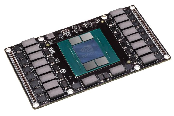
Just as the Volta GPU was expected to, Pascal will have “3D stacked memory”—memory chips stacked one on top of the other and joined by circuitry, resulting in graphics cards that can access up to 1 terabyte per second (TBs) of bandwidth. The 1TB/s threshold will be achieved by stacking memory on top of the GPU itself, with a silica substrate between them, and then cutting a hole through the silicon to connect each layer. Nvidia’s current GPUs can access only 288GB/s; upcoming Pascal graphics cards, then, will be about 3.5 times faster.
According to Nvidia’s CEO, Jen Hsun-Huang, 1TB/s is fast enough to move “all of the data from a full Blu-Ray disc through the chip in 1/50th of a second.” It should be noted, though, that manufacturing GPUs with a terabyte of DRAM on them would make for some rather expensive graphics cards. Nvidia says that how much memory the Pascal cards will actually contain will come down to cost. Also, one must consider how much bandwidth are graphics card buyers willing to shell out for?

Moving all that data
At this point, the current PCI-Express bus standard, or even the up-coming PCIe 4.0 standard, are not beefy enough to handle all this bandwidth. To compensate, Nvidia has come up with its own bus technology, dubbed NVLink.
Basically, NVLink provides a bigger pipe between the GPU and the CPU, and therefore, a much bigger data path, at least by today’s (or the immediate future’s) standards. For example, PCIe 3.0 transfers data at an impressive 8 gigatransfers per second (GTs), while Nvidia’s NVLink is expected to move data at about 20GTs, which is over twice as fast.
Unlike the PCIe bus, which is essentially a discrete switch built into the CPU, NVLink is a direct, or point-to-point, connection between the GPU and the CPU. In this way, NVLink is similar to Intel’s Quick Path Interconnect (QPI), or AMD’s Hypertransport.
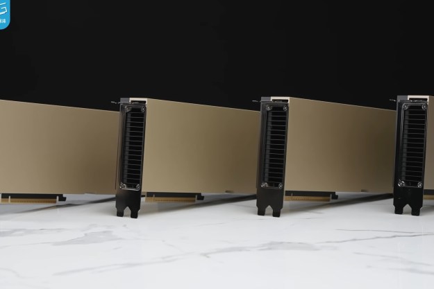
However, as you can imagine, to pull off these massive data transfers, the current PCIe connectors aren’t adequate. To compensate, Nvidia has come up with what it calls a mezzanine connector, which is the same type used to link multiple printed circuit boards (PCBs). Think of a socketed GPU, similar in concept, to a CPU connection.
Another drawback is, of course, dramatically redesigned motherboards. Most game enthusiasts, and perhaps even some imaging, digital video, and 3D graphics and animation professionals, would probably consider this a small price to pay to accommodate the essential doubling of graphics data bandwidth.
Will Pascal take off once it hits the market? As is usually the case, one of the biggest, if not the biggest, determining factor will be price.
Editors' Recommendations
- I was wrong — Nvidia’s AI NPCs could be a game changer
- At this point, we know just about everything about Nvidia’s new GPUs
- Why it’s a surprisingly good time to buy a GPU right now
- This AMD GPU could have destroyed Nvidia, but we might never see it
- Nvidia doesn’t want you to know about its controversial new GPU