
World’s first 2nm chip could quadruple battery life with a quarter of the energy

IBM Unveils World's First 2 Nanometer Chip Technology

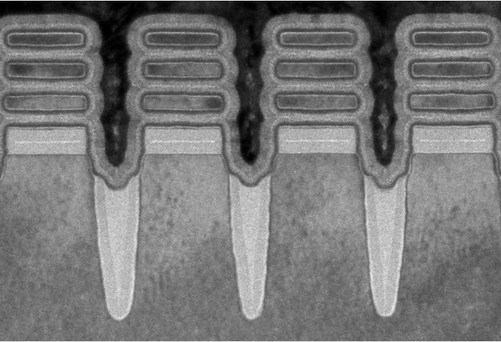
IBM unveiled the world’s first 2nm chip technology on Thursday, setting a new bar for the semiconductor industry. The new design can fit up to 50 billion transistors on a chip the size of a fingernail, which Darío Gil, SVP and Director of IBM Research, says is  “essential to the entire semiconductor and IT industry.” IBM claims the new design can achieve 45% high performance and 75% lower energy use compared to chips using a 7nm process.

In real-world use, that could mean quadrupling cell phone battery life, requiring a charge only every four days, speeding up object detection in self-driving cars, and improving the speed and efficiency of laptops. IBM was able to achieve this new process by utilizing Gate-All-Around (GAA) stacked nanosheets, helping push beyond the typical FinFET manufacturing process.

2nm technology as seen using transmission electron microscopy. 2nm is smaller than the width of a single strand of human DNA. Courtesy of IBM.

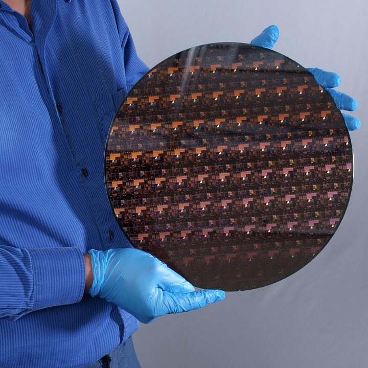
2nm is a new low (in a good way) for the semiconductor industry. Manufacturer TSMC offers a 5nm process currently and is currently researching 2nm production, and Samsung showed off a 3nm chip earlier this year. Unlike TSMC and Samsung, though, IBM doesn’t manufacture anything. This “breakthrough” comes from IBM’s Albany Nanotech Complex in Albany, NY, where the company researches future semiconductor technology.

That said, IBM has a few strategic partnerships. In 2014, the company signed a 10-year manufacturing agreement with the New York-based GlobalFoundries. More recently, IBM announced partnerships with Samsung and Intel. Although the new design will benefit the semiconductor industry as a whole, it could help bolster U.S. manufacturing, especially as Intel tries to expand its production capacity.

A 2nm wafer fabricated at IBM Research’s Albany facility. The wafer contains hundreds of individual chips. Courtesy of IBM

From IBM’s view, the collaborative effort is what made this achievement possible. “It is the product of IBM’s approach of taking on hard tech challenges and a demonstration of how breakthroughs can result from sustained investments and a collaborative R&D ecosystem approach,” Gil said.

You shouldn’t expect to see chips using the 2nm process anytime soon, however. The energy-efficient design will likely make its way into manufacturing plants and data centers first. First, maybe, but not soon. IBM’s achievement still comes amid a disastrous global semiconductor shortage that may not fully recover until 2023.

Editors' Recommendations

Jacob Roach
Senior Staff Writer, Computing
Jacob Roach is a writer covering computing and gaming at Digital Trends. After realizing Crysis wouldn't run on a laptop, he…
Meet the world’s first 2D material: 5 ways Graphene could transform your phone
Quantum Hydrogen on Graphene

Graphene is the world’s first two-dimensional material. It is one atom thick, which makes it a million times thinner than a human hair. It is also very strong, flexible, transparent, and more conductive than anything else we know. The potential applications are seemingly endless -- and the first examples are close to fruition.

There are many, many projects worldwide investigating the potential of graphene for a wide variety of industries, but there are compelling reasons for mobile technology manufacturers in particular to sit up and take notice. Researchers from Samsung and Nokia were among the speakers at the recent Graphene Supply, Application & Commercialisation 2014 summit in Manchester, discussing the feasibility of mass production, the need for further investment, and potential applications ranging from flexible touch screens to transistors and semiconductors.
A brief history
Graphene has been on the horizon for decades. It was first studied at a theoretical level back in the late 1940s, but it wasn’t practically pursued until the 1970s. Millions of layers of graphene form graphite, which is used in pencils, but scientists couldn’t figure out how to isolate it.

Read more
The biggest Mac announcement at WWDC was about the old MacBook Air
15-inch MacBook Air shown at WWDC 2023.

Apple announced a ton of new Macs at WWDC 2023, including the 15-inch MacBook Air and a long-awaited update to the Mac Pro. However, the biggest announcement of the event flew under the radar, and it has to do with the older 13-inch MacBook Air.

Introducing the 15-inch model, Apple announced that it's slashing the price on the 13-inch M2 MacBook Air by $100, bringing it down to $1,100. It's still not as cheap as the M1 MacBook Air, which comes in at $1,000, but it's much closer.

Read more
MacBook Air 15-inch vs. MacBook Pro 14-inch
macbook air 15 inch vs pro 14 front view

Apple introduced a brand-new member to its MacBook lineup, a larger MacBook Air model with a 15.3-inch display that utilizes the same base M2 processor as the latest MacBook Air 13. The idea, clearly is to provide a larger laptop that retains the incredible thinness and lightness of the MacBook Air, but with more screen real estate to work with.

In this comparison, it's going up against the MacBook Pro 14, with a display that's about an inch smaller diagonally at 14.2 inches. The thing is, the MacBook Pro 14 is in a different class entirely when it comes to performance, with M2 Pro and M2 Max CPUs, as well as a truly stunning Mini-LED panel. Which one is right for you?
Specs

Read more