Intel unveiled a road map through 2025 at its Intel Accelerated event on Monday. Beyond showing what’s coming down the pike, Intel announced that it would overhaul its naming scheme to move past the nanometer (nm) measurement used by the rest of the industry. Going forward, Intel will classify each improvement in process technology with a simple name.
Previously, Intel abided by the industry naming scheme of process node advancements. Measured in nanometers, each new generation marked an uptick in the density of transistors on the chip, not its physical size. The name is largely irrelevant at this point and has morphed into a marketing ploy by chipmakers like Samsung and TSMC.
As advancements were made in density, the rest of the industry simply brought the number down. So, 10nm moved to 7nm, and so on. Intel didn’t. Instead, Intel kept with its 14nm name for quite some time, as the company experienced issues moving on to a 10nm process node.
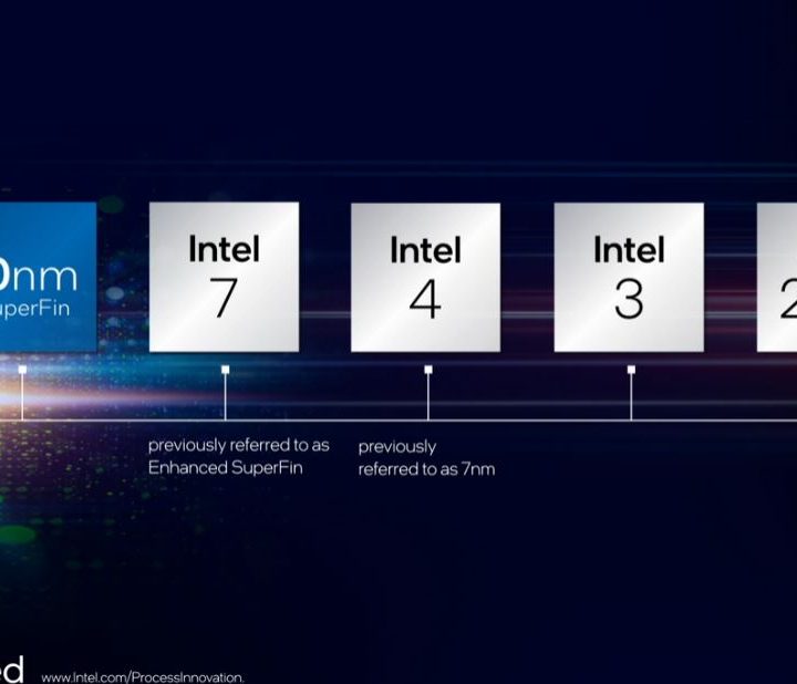
Now, Intel has brought the scales back in balance. Starting with Alder Lake processors, which are set to launch later this year, Intel will use a number that more accurately represents its transistor density compared to the rest of the industry. That starts with Intel 7 on Alder Lake, which was previously known as 10nm Enhanced.
Following up Intel 7 is Intel 4, which was previously referred to as Intel 7nm and will show up on Meteor Lake processors in 2023. After that is Intel 3, and after that is Intel 20A, where the company will break the naming scheme and usher in the “angstrom era,” where manufacturing processes will move beyond 1nm.
Here’s what you can expect from each process improvement:
- Intel 7 (previously 10nm Enhanced) – “Delivering an approximately 10% to 15% performance-per-watt1 increase over Intel 10nm SuperFin through FinFET transistor optimizations, including increased strain, more low-resistance materials, novel high-density patterning techniques, streamlined structures, and better routing with a higher metal stack.”
- Intel 4 (previously Intel 7nm) – “Providing an approximately 20% performance-per-watt1 increase over Intel 7, Intel 4 is the first Intel FinFET node to fully embrace extreme ultraviolet lithography (EUV). Intel 4 will be ready for production in the second half of 2022 for products shipping in 2023, including Meteor Lake for client and Granite Rapids for the data center.”
- Intel 3 – “Continuing to reap the benefits of FinFET, Intel 3 is expected to deliver around an 18% performance-perwatt1 increase over Intel 4. Intel 3 will be ready to begin manufacturing products in the second half of 2023.”
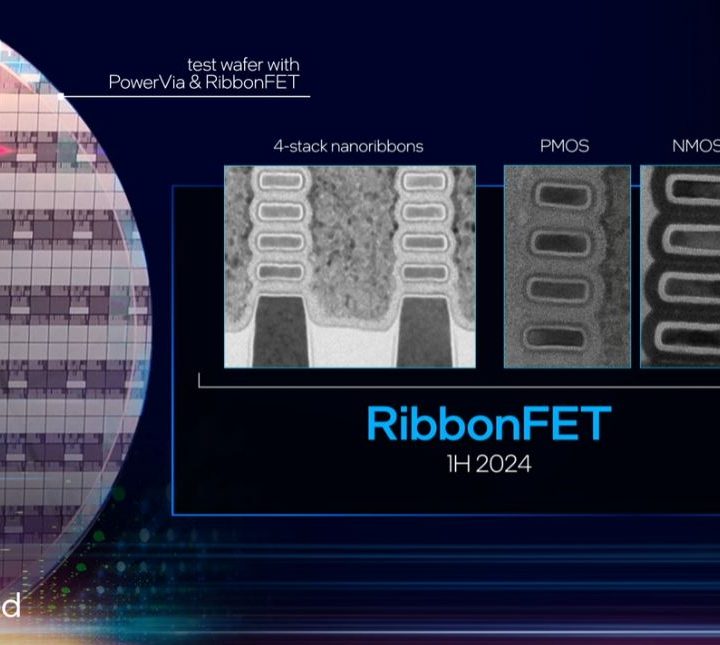
- Intel 20A – “Ushering in the angstrom era with two breakthrough technologies, PowerVia and RibbonFET. Intel 20A is expected to ramp in 2024.”
After Intel 20A, the company will move to Intel 18A as it continues the downward trek once again. Intel 18A is already in development for early 2025, featuring refinements to RibbonFET.
How Intel will go beyond 1nm
The “angstrom era” will begin with Intel 20A, which utilizes two new technologies that the company announced at the Intel Accelerated event. The first is PowerVia, which is an “industry-first implementation of backside power delivery.” Instead of routing power through the front of the wafer, PowerVia routes it through the back, optimizing the signal routing and improving efficiency.
RibbonFET is the name Intel is using for its gate-all-around (GAA) transistor design. It’s the first new design the company has unveiled since it introduced FinFET in 2011, and it will further improve transistor switching to deliver faster, more efficient processors. This design essentially utilizes multiple gates on the transistor, allowing it to switch faster compared to a single gate.
Intel 20A would have otherwise been known as Intel 1, but the company changed the name to “better evoke the next era of innovation.” This is where Intel will move beyond 1nm while continuing to keep with the idea of Moore’s Law, where transistor density doubles every two years.
“Moore’s Law is alive and well. We have a clear path for the next decade of innovation to go to ‘1’ and well beyond. I like to say that, until the periodic table is exhausted, Moore’s Law isn’t over and we will be relentless in our path to innovate with the magic of silicon,” Intel CEO Pat Gelsinger said.
Pushing beyond the nanometer
Intel’s shift to a new naming convention may not seem like much — and for many, it doesn’t mean anything. At best, the move shows just how meaningless process naming conventions are, as they mark generational shifts more than where different chipmakers are at in terms of innovation.
But it means a lot for Intel Foundry Services (IFS). IFS is Intel’s plan to provide manufacturing capacity to other businesses. At the Intel Accelerated event, the company announced its first partnership with Amazon Web Services, as well as a partnership with Qualcomm with Intel 20A.
As Intel tries to grab customers from rival chipmakers Samsung and TSMC, the change in naming reflects what the company is able to deliver in terms of transistor density. It highlights how arbitrary the measurement has been over the past several years and tips the scales back in Intel’s favor, if only by a bit.
Although Intel’s shift in naming is the biggest news to come out of the event, the company also touched on the Foveros Omni and Direct packaging technologies, which will build on the Foveros packaging technology featured in Alder Lake and Meteor Lake. Intel still has a long road back to the top, but the change shows that it’s willing to take the steps.