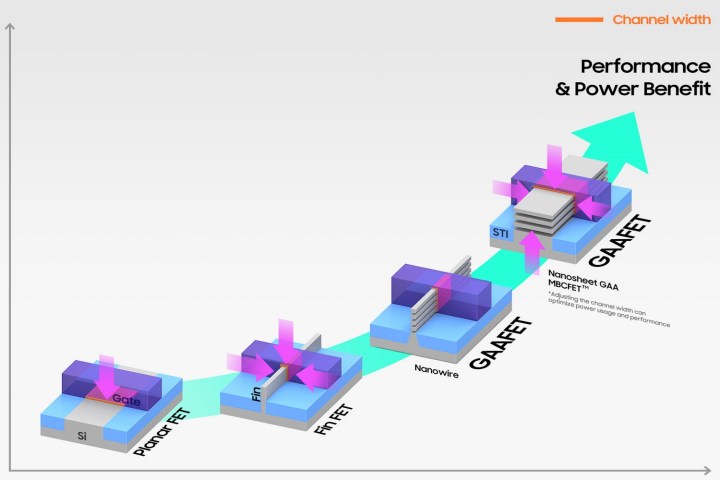
Samsung says it has begun mass production of faster and more efficient chips based on the 3-nanometer process, becoming the world’s first company to do so and gaining a market lead over key rival TSMC. Samsung is using the new GAA (Gate-All-Around) tech to make the 3nm chips, bringing some notable improvements to the table.
Take for example the current crop of mobile processors such as the Tensor SoC inside the Pixel 6 series, which is based on Samsung’s 5nm process node. Compared to the 5nm process, Samsung says the first-generation 3nm process upgrade will offer a 23% jump in performance while consuming 45% less power. As refinements happen over time and the second-generation 3nm process is developed, the performance gain will touch the 30% mark, while power efficiency will increase to 50%.
Samsung is starting the first application of the nanosheet transistor with semiconductor chips for high performance, low power computing application and plans to expand to mobile processors.
— Samsung Semiconductor (@SamsungDSGlobal) June 30, 2022
Samsung is initially targeting the 3nm-based chips at “high performance, low power computing application” customers and will eventually expand to mobile processors. However, the company hasn’t said when the first mobile SoC based on the 3nm process will make its way to a smartphone or PC.
Why care about nanometers?
When it comes to processors, the nanometer figure advertised by chipmakers and consumer electronics brands broadly refers to the size of transistors. These transistors are the fundamental computing units for a processor, just the way plant cells act as the individual energy generation factories for plants. Modern-day processors have billions of transistors packed on a tiny wafer, which turn on and off via electrical signals to perform calculations.

The higher the number of transistors you can fit on a chip, the more powerful it gets. But for gadgets like a phone or a smartwatch, space inside is at a premium. To overcome the space constraint, transistors need to be miniaturized. As the fabrication process shrinks the size at the nanometer scale, the transistor density increases, offering more power and improving efficiency at the same time.
In a nutshell, the smaller the nanometer figure for a chip, the higher the performance and efficiency. It’s an important area of development for key players like TSMC, Intel, and Samsung, as they all battle to deliver more powerful products. Here, Samsung has just taken a notable lead.
What’s in the future for Samsung?
Samsung’s chip foundry makes processors for its own gadgets, such as the Exynos 1280 chip found inside the Galaxy A53 5G, plus it offers chip fabrication services to clients like Google. So far, Samsung has not revealed the name of clients that will avail its 3nm chip fabrication services.
While Samsung’s achievement is remarkable, the road ahead won’t be easy, especially when it comes to pocketing rich clients like Apple and Qualcomm. Not only does Samsung have to undercut TSMC in terms of pricing, but it will also have to demonstrate that its 3nm chip fabrication process is more efficient and can handle volume orders better than TSMC’s own 3nm offering, which is slated to enter mass production in the second half of 2022. Beyond that, TSMC currently has plans to make 2nm chips in 2025.
As nodes get smaller and performance needs grow greater, IC designers face challenges in handling tremendous amounts of data to verify complex products with more functions and tighter scaling.
— Samsung Semiconductor (@SamsungDSGlobal) June 30, 2022
Samsung’s own Exynos chips have sometimes failed to match the prowess of competing processors made by TSMC for years, despite matching the fabrication process at the nanometer scale. But Samsung has lately been making positive strides. Last year, the company announced plans to pour $132 billion into its logic chip and foundry business by the end of 2030. Additionally, it is leveraging AMD’s expertise in making GPUs for its mobile processors, giving them an added dash of graphics grunt to handle demanding tasks like games. It remains to be seen whether 3nm is finally the turf that allows Samsung to catch up with TSMC, or even go on to surpass it.
Editors' Recommendations
- Samsung’s new fitness tracker could be released any day now
- Samsung may have made a horrible decision with the Galaxy S24
- There’s a big problem with Samsung’s new Android tablets
- MediaTek’s Dimensity 9200 chip is packed with world’s-first tech
- Samsung’s new 200MP smartphone camera looks incredible


