Although Moore’s Law hasn’t been strictly maintained in recent years, the steady improvement in processor performance and reductions in their size has continued. However, as we edge towards the 10nm die size, yield issues have become increasingly common. Most expect big changes will be required to continue to shrink the size of new microprocessors and this new method could go some way to aiding that.
Developed by post-doctorate Do Han Kim, graduate student Priya Moni, and Professor Karen Gleason of MIT, and post-doctorate Hyo Seon Suh and Professor Paul Nealey from the University of Chicago, the new technique uses common manufacturing techniques, but in new and novel ways.
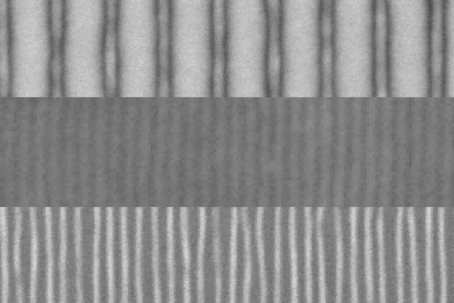
The first part of the process involves creating a pattern of lines on the chip surface, using standard lithographic techniques — an electron beam essentially prints the pattern onto the chip. The next step puts down a layer of two different polymer materials which are laid down in the original patterns. It’s those polymers which will attract the final layer using vapor deposition.
That process involves heating precursors so they evaporate and then allowing them to condense on the chip. This process forces the copolymers to form into vertical layers rather than horizontal ones and in actuality, form far thinner lines than their bases. New layers can be formed atop the initial one, creating a much thinner, interconnected chip than is created by traditional manufacturing techniques.
This could allow for the much more simple creation of sub-10nm components, which was seen as the next big barrier in computing.
Most importantly, this utilization of traditional chip manufacturing methods in a novel fashion means that existing fabrication plants don’t need to be refitted to make use of the technique. The question now is whether it can be repeated on a mass scale. MIT is confident that it can and that it will be economically viable as well.
Editors' Recommendations
- DuckDuckGo’s new browser could help keep Mac users safe on the web
- Intel reports new computing breakthroughs as it pursues Moore’s Law
- MIT’s tiny walking robot could eventually build other, bigger robots