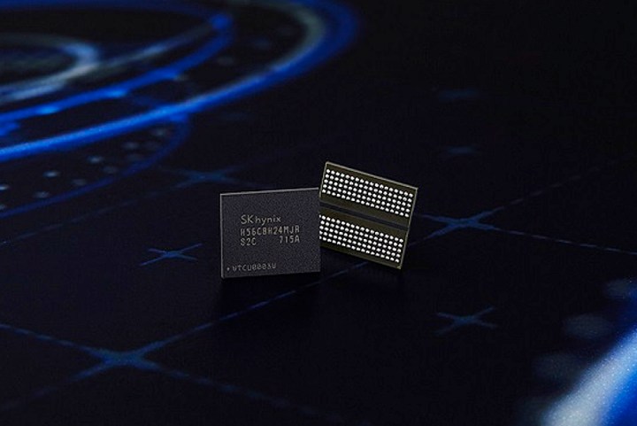
SK Hynix said that its upcoming 8Gb memory chips will be manufactured using 2Xnm process technology, meaning anywhere between 20nm and 29nm. Each chip will also have an I/O data rate of 16 gigabits per second per pin, making it the “world’s fastest” to date. Throw in a 384-bit memory interface, and the GDDR6 tech will have the ability to process up to 768GB of graphics data per second. As a reference, GDDR5X memory used on the GeForce GTX 1080 Ti has an I/O transfer rate (bandwidth) of under 500GB per second.
“GDDR6 is a next generation graphics solution under development of standards at JEDEC, which runs twice as fast as GDDR5 having 10 percent lower operation voltage,” the company said. “As a result, it is expected to speedily substitute for GDDR5 and GDDR5X. SK Hynix has been collaborating with a core graphics chipset client to timely mass produce the GDDR6 for the upcoming market demands.”
Current memory chips based on GDDR5 have 170 pins, 67 of which are specifically used for the I/O data exchange while the others are for grounding and power purposes. The more recent GDDR5X builds on that design by adding 20 pins to the form factor, providing an additional I/O boost. SK Hynix’s GDDR6 appears to have 180 pins.
The major difference between GDDR (Graphics Double Data Rate) and HBM (High Bandwidth Memory) is similar to what divides regular NAND and 3D NAND. On the GDDR5 front, chips are spread out horizontally in physical space, limiting the actual size of the graphics card and requiring “larger voltage circuity.” HBM tech takes the skyscraper approach by stacking memory chips vertically, which in turn provides better I/O bandwidth.
As for that “core graphics chipset client” comment, we’re betting it’s Nvidia. The company’s next-generation graphics chip architecture, code-named Volta, will supposedly use GDDR6 memory technology in 2018. The current crop of Pascal-based “GeForce” graphics cards for the gaming market use GDDR5 and GDDR5X while Nvidia’s “Tesla” solutions for the enterprise sector use HBM2 tech.
Meanwhile, AMD fully backs HBM technology, which was used on its Fuji-based graphics cards for the gaming market in 2015. AMD is also getting ready to unleash new


